NAPA works on the develoment of a novel variant of SPR-Surface Plasmon Resonance – based optical detection. Several market available sensor devices using plasmon excitation/detection have proven high sensitivity gaseous pollutant and chemical contaminants sensing with, however, modest selectivity. Most of them are still cumbersome, and their complexity limits large scale deployment. The development of a sensor which is compact, easy to implement, robust, power sparing, sensitive and selective to a given molecule represents a technical challenge which is the object of several industrial R&D projects.
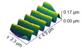
AFM micrograph of a linear diffraction grating
The surface plasmon mode is a propagating evanescent wave confined at a metal-dielectric interface having a strong electrical field at the interface. This field is therefore highly sensitive to any variation of complex refractive index at, or close to the interface, for instance that of a transducing nanolayer deposited at the interface. These changes (refractive index and/or nanolayer thickness) can be induced by the adsorption (chemisorption, physisorption) of gaseous or liquid pollutants. NAPA is working on applying this technology to O3, H2S and H2 sensing
SERS Sensors
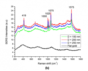
Raman Spectroscopy is an efficient analysis technique to characterize chemical composition of molecules, relying on inelastic light scattering. Nevertheless, for low concentration it gives very weak signal. To overcome this limitation, metal nanostructures can be used. This method is called Surface Enhanced Raman Scattering (SERS) and thus permits precise identification of the molecules thanks to their specific peaks and high enhancement factors. The interest to develop new SERS-based spectroscopic sensors for chemical or biological applications increased in the past few years.
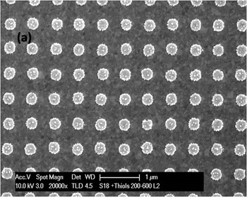
Gold nano pillars on glass surface for SERS detection
SERS measurements with pitch 400 nm and diameters 150-250
To pattern such device two kinds of lithographic processes can be used:
conventional electron beam lithography (EBL) which needs long writing times for large areas and a significant cost for large sample productions.
NIL, which is rapid, with low cost fabrication, and allows large area structuring.
Thanks to this technology, molecular detection of diluted compounds is possible down to ppm.